
How AI is helping Indian semiconductor startups speed up design cycles has become one of the most important shifts in the country’s deep tech ecosystem. As India pushes to build a domestic chip design and manufacturing base, artificial intelligence is reducing time, cost, and complexity across the semiconductor development process.
For startups operating with limited capital and aggressive timelines, AI is no longer an optional enhancement. It is becoming a core design tool that enables faster iterations, fewer errors, and quicker paths from concept to tape out.
Why Semiconductor Design Cycles Are Traditionally Slow
Semiconductor design is one of the most complex engineering processes. Chip development involves multiple stages such as architecture design, logic verification, physical layout, power optimization, and testing. Each stage depends heavily on manual expertise and repeated simulations.
Traditionally, design cycles can take 18 to 36 months, especially for advanced nodes. Errors discovered late in the process can force costly redesigns. For Indian startups competing with global players, long cycles increase burn rates and delay market entry.
This is where AI driven automation is changing the equation by compressing timelines without compromising accuracy.
AI Driven Chip Architecture Exploration
One of the earliest impacts of AI in semiconductor startups is in architecture exploration. AI models can analyze thousands of design configurations and performance trade offs far faster than human teams.
Instead of relying on fixed templates, startups use AI to simulate workloads, predict bottlenecks, and recommend optimized architectures based on target applications such as automotive, telecom, or edge AI.
This helps teams converge on viable designs earlier, reducing the trial and error that traditionally consumes months. Faster architectural decisions directly shorten the overall design cycle.
Accelerating Verification and Testing with AI
Verification is often the most time consuming phase in chip design. Ensuring that a design behaves correctly across all scenarios requires extensive testing and simulation.
AI tools help by identifying high risk areas in the design and prioritizing test cases accordingly. Machine learning models learn from past verification data to predict where failures are most likely to occur.
For Indian semiconductor startups, this targeted verification approach reduces simulation workloads and speeds up bug detection. Faster verification means fewer late stage surprises and smoother tape out schedules.
AI in Physical Design and Layout Optimization
Physical design involves placing and routing billions of transistors while balancing power, performance, and area constraints. This step traditionally requires multiple manual iterations.
AI algorithms now assist in layout optimization by learning from previous designs and predicting optimal placement strategies. These tools can automatically adjust routing to minimize signal delays and power leakage.
By reducing the number of manual layout revisions, AI shortens physical design timelines significantly. Startups benefit from quicker design closure even with smaller engineering teams.
Improving Power Efficiency and Yield Prediction
Power efficiency is a critical concern, especially for chips targeting mobile, automotive, and edge devices. AI models analyze power consumption patterns early in the design phase and suggest improvements.
AI is also used to predict manufacturing yield based on design parameters. By identifying design choices that may lead to lower yields, startups can make corrective changes before fabrication.
This proactive optimization saves time and cost by reducing the risk of post fabrication failures, which can otherwise set projects back by months.
Reducing Dependency on Large Engineering Teams
Indian semiconductor startups often operate with lean teams compared to global giants. AI tools help bridge this gap by automating repetitive and computation heavy tasks.
Design automation allows smaller teams to handle complex projects that previously required large specialized groups. This efficiency is crucial for startups managing both time and capital constraints.
As a result, startups can move faster from concept to prototype without scaling headcount proportionally.
Enabling Faster Iteration and Custom Chip Design
AI enables rapid design iteration, which is especially valuable for startups building application specific integrated circuits. Custom chips often require multiple refinements to meet customer needs.
Machine learning models analyze performance feedback and suggest design tweaks automatically. This allows startups to iterate designs quickly and respond to client requirements without restarting the entire design flow.
Faster iteration cycles improve customer confidence and shorten sales timelines.
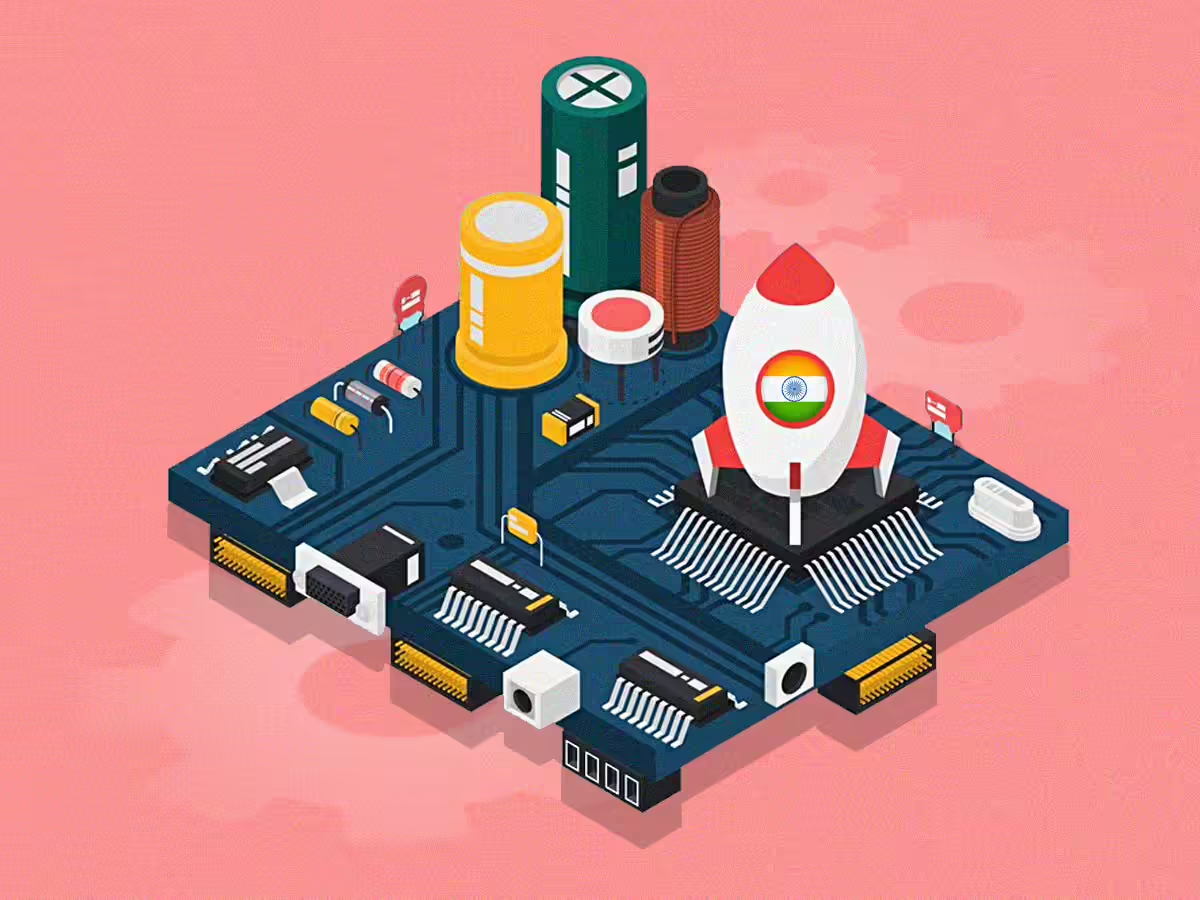
Strengthening India’s Semiconductor Ecosystem
How AI is helping Indian semiconductor startups speed up design cycles also has ecosystem level implications. Faster design cycles attract global customers, strategic partnerships, and investor interest.
AI driven efficiency aligns with national goals to build a competitive semiconductor industry. It enables Indian startups to participate meaningfully in global supply chains despite limited access to advanced fabrication facilities.
As AI tools mature, design capability becomes less dependent on geography and more on innovation.
Challenges and Limits of AI Adoption
Despite the benefits, AI adoption in semiconductor design is not without challenges. High quality training data, integration with existing electronic design automation tools, and trust in AI driven decisions remain concerns.
Startups must also ensure that AI recommendations align with real world manufacturing constraints. Human oversight remains essential.
However, these challenges are gradually being addressed as AI models improve and industry standards evolve.
The Road Ahead for Indian Semiconductor Startups
AI will continue to compress design timelines further as tools become more specialized and accessible. Startups that adopt AI early gain a structural advantage in speed and efficiency.
Future design cycles are likely to be measured in months rather than years for many categories of chips. This shift could redefine India’s role in the global semiconductor landscape.
The combination of AI, skilled talent, and focused application markets positions Indian startups for sustained growth.
Takeaways
- AI significantly reduces semiconductor design cycle timelines
- Verification, layout, and power optimization benefit the most
- Lean startup teams gain capabilities comparable to larger players
- Faster design cycles strengthen India’s semiconductor ecosystem
FAQs
Why are semiconductor design cycles traditionally long?
They involve complex multi stage processes with heavy reliance on manual verification and repeated simulations.
Which design stages benefit most from AI?
Architecture exploration, verification, physical layout, and power optimization see the biggest time savings.
Can AI replace chip design engineers?
No. AI augments engineers by automating repetitive tasks, but human expertise remains critical.
Does AI reduce design costs for startups?
Yes. Faster cycles and fewer errors lower development costs and reduce capital burn.